
SALVE - Cs/Cc corrector for TEM (low-kV range)
SALVE - Cs/Cc corrector for TEM (low-kV range)
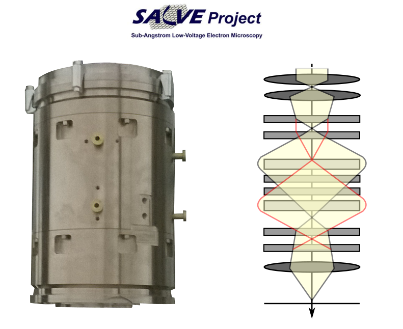
The abbreviation SALVE stands for Sub-Angstrom-Low-Voltage-Electron microscope (www.salve-project.de), which is a research project of the University of Ulm, the company ThermoFisherScientific and the company CEOS. Therein, a special Cc/Cs-corrector was developed by CEOS for special use in low-voltage transmission electron microscopy in the range from 20 kV to 80 kV. The limitation to low accelerating voltages is extremely important to avoid damage in electron beam sensitive objects. The SALVE Cc/Cs-corrector is a quadrupol-octupole-corrector, which eliminates not only the 3rd order spherical aberration Cs=C3 but also the off-axial coma B3, and moreover corrects for the linear chromatic aberration Cc. The correction of Cc requires not only magnetic multipole fields but also very strong electrostatic quadrupole elements (up to +/- 8kV). CEOS is the only company world-wide, which successfully applies this elaborate technology for aberration correction in TEM. The optical design additionally allows for a complete correction of all axial aberration up to including 5th order as well as all off-axial aberrations up to including 3rd order. The intrinsic (+) spherical aberration of 5th order (C5) of the SALVE corrector was carefully optimized for ideal phase contrast imaging conditions for a large aperture angle of at least 50 mrad. This enables high-contrast imaging of light atoms (weak phase objects) over the whole high voltage range.The correction of the chromatic aberration Cc does not only considerably improve the TEM's information limit (resoving power), but also enables a much higher image contrast due to the additional contrast contribution of inelastically scattered electrons which only form a blurred image background in Cc-uncorrected images.For these reasons, the SALVE Cc/Cs-corrector is the ideal equipment for high-resolution TEM investigations on electron beam sensitive objects like graphene or bio-molecules, as well as for spectroscopic imaging (EFTEM).
You can find more information about the SALVE corrector in our publication:
and on www.salve-project.de
(+) intrinsic aberrations = aberrations that occur and are unavoidable due to the optical design of the corrector.
Features:
- Quadrupole-octupole type corrector for low-voltage TEM
- Simultanious correction of the chromatic aberration Cc, the spherical aberration Cs=C3 and the off-axial coma B3
- Ajustable for the high-voltage range from 20 kV up to 80 kV.
- Correction of all axial aberrations up to 5th order (A1, B2, A2, C3, S3, A3, B4, D4, A4, C5, S5, R5, A5).
- Corrects off-axial aberrations up to including 3rd order(A1g/G, A2g/G, B2g/G)
- Optimized sphercial aberration of fifth order (C5) for ideal phase contast imaging conditions for an optical aperure of at least 50mrad over the whole high-tension range
- Compared to the use of a monochromator for resolution improvment Cc correction offers a much more intense electron beam at the same or better image resolution and therefore allows much shorter exposure times hence higher throughput.
- Higher image contrast due to additional high-resolution contrast contribution from inelastically scattered electrons by Cc correction.
- Less knock-on damage on electron beam sensitive samples and, at the same time, highest resolution imaging, due to the combination of low acceleration voltage with Cc/Cs-correction.
- Compatible with the following TEMs: TFS (TitanTM Themis)
Specifications:
- Device dimensions: 468 x 560 x 560 [mm]
- Mode: TEM
- High voltage range: 20kV – 80kV
- Target resolution: Proper phase contrast imaging conditions to at least 50 mrad aperture angle. Experimental reolution at different high-tensions:
- 62 mrad (Aperture angle) - 20 kV (High voltage) - 139 pm (Information limit)
- 61 mrad (Aperture angle) - 30 kV (High voltage) - 115 pm (Information limit)
- 67 mrad (Aperture angle) - 40 kV (High voltage) - 90 pm (Information limit)
- 59 mrad (Aperture angle) - 60 kV (High voltage) - 83 pm (Information limit)
- 55 mrad (Aperture angle) - 80 kV (High voltage) - 76 pm (Information limit)
Applications:
- High-resolution TEM for electron beam sensitive samples at low accelerating voltages (20kV – 80kV), e.g. thin and light materials such as graphene, lithium compounds or bio-molecules
- Spectroscopic imaging (EFTEM)
Contact:
Do you have any questions about the product or the application and extension for your e-beam system? Please contact us at info@ceos-gmbh.de
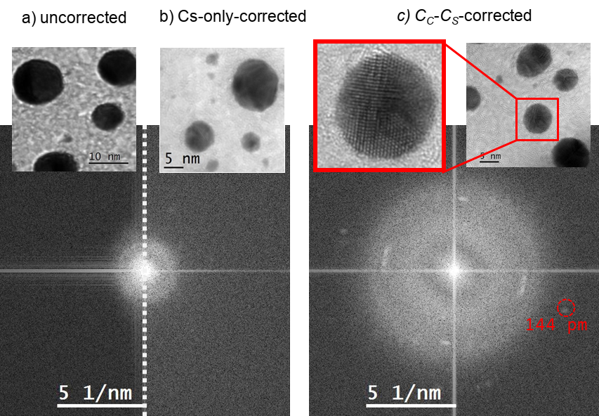
20kV TEM images of gold particles on carbon film and the corresponding diffractograms: (a) In the uncorrected TEM, both, chromatic and spherical aberration dramatically limit the micorscope resolution. Therefore, only large area contrast is resolved. (b) Cs-correction does only slightly improve the resolving power because the chromatic aberration Cc strictly dominates the resolution limit at low high-tensions. (c) Simultanious Cc/Cs-correction in the SALVE microscope allows for true atomic resolution of the gold particles at only 20kV. The diffractogram shows the Au [022] reflections, which correspond to the 144pm lattice distance. Linck et al. PRL 117, 076101 (2016).
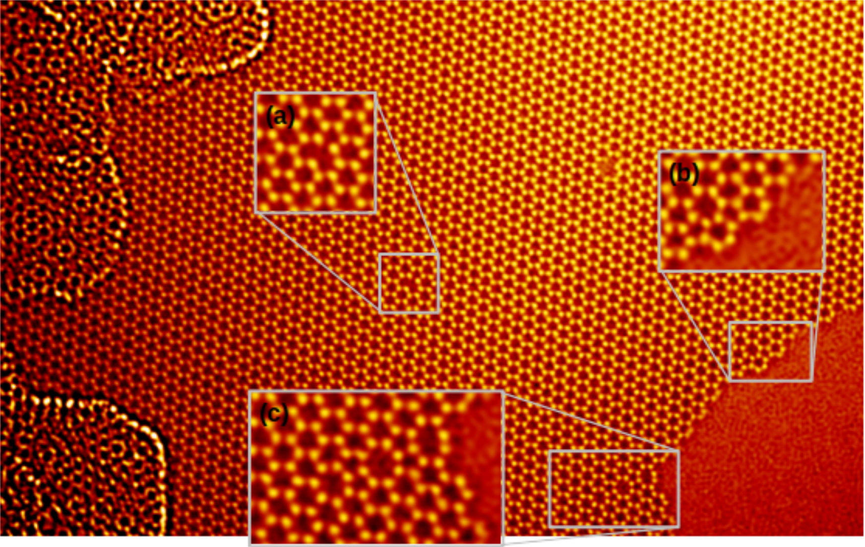
Cc-Cs-corrected phase contrast TEM image of a carbon monolayer (graphene) at 80kV. Although single carbon atoms are very weak-scattering objects, they can be imaged with strong contrast and high spatial resolution in the Cc-Cs-corrected SALVE microscope. The individual atoms are sharply resolved within the characteristic hexagon graphene structure over a large area. This is only possible with low beam energies, because above 80kV the carbon atoms can be “kicked-out” from the graphene lattice (knock-on damage). Consequently, various defects can be monitored which are otherwise unstable at higher beam energies. As an example, in subimage (a) one individual carbon atom is missing; at higher beam energy a hole would grow very quickly. (b) At the edge of the graphene layer different structures, which differ from the hexagon, can be observed. The example shows carbon rings consisting of five and seven carbon atoms instead. (c) In case the graphene lattice is slightly rotated in plane, grain boundaries are formed, where alternately five and eight atoms are arranged within one carbon ring to adjust the differently oriented neighboring graphene areas.
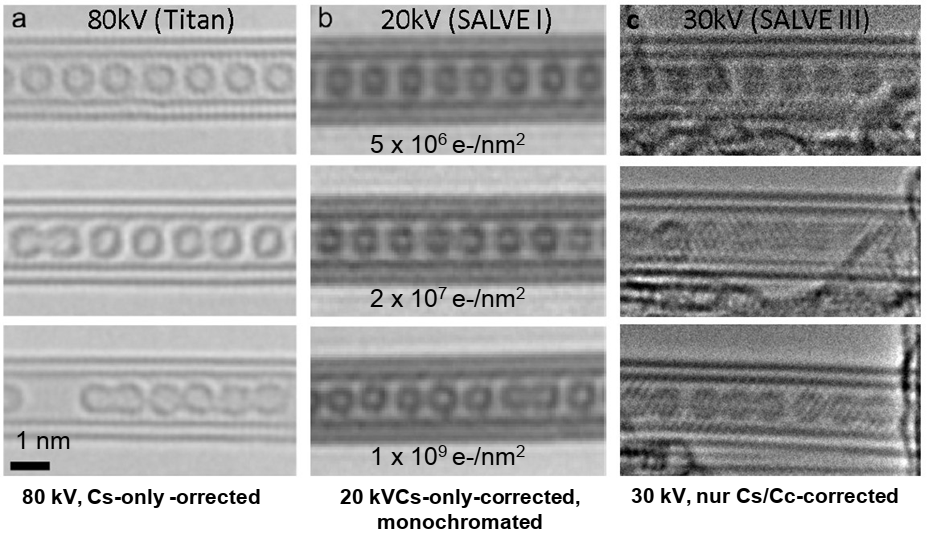
Dose-dependent experiments on C60 molecules in double-wall carbon nanotubes (CNTs): from top to bottom row the electron dose on the sample increases by several orders of magnitude. (a) Cs-correction at 80kV allows to resolve atomic details. However, the C60 molecules are already damaged at moderate dose. (b) At 20kV The C60 molecules remain stable at higher doses, but Cs-correction alone is not sufficient to establish atomic resolution. (c) Simultanious Cc/Cs-correction enables atomic-resolution imaging also at very low accelerating voltages: in the example the C60 molecules as well as the CNT double-wall are clearly resolved on the atomic level at only 30kV (even better than in (a) ) and they remain stable at very high electron doses.
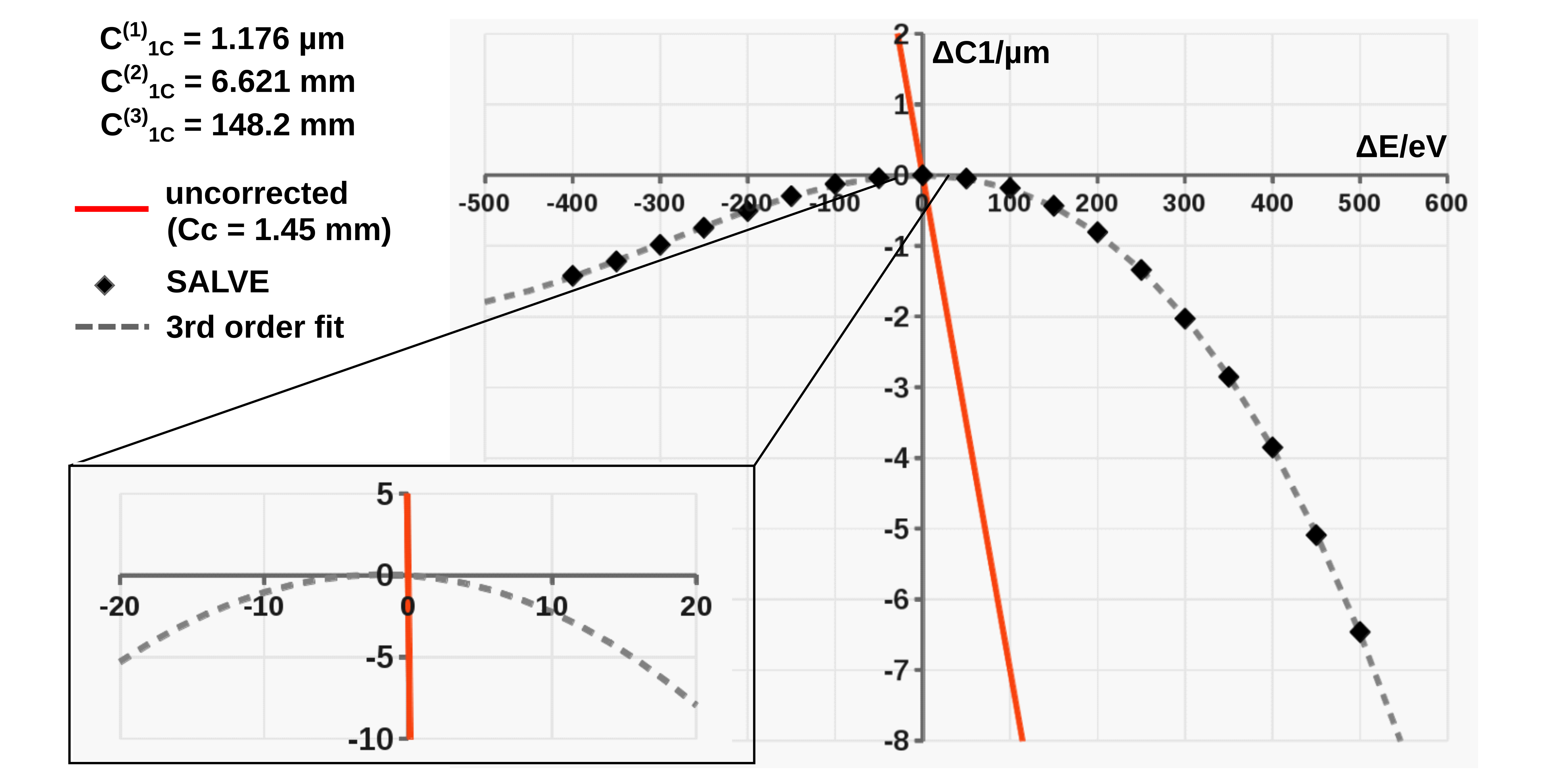
The chroamtic aberration (energy-dependent defocus) can be expanded to a power series with respect to the chromatic parameter κ = ΔE/E: C1 = - Σ jC1c (j)κj. After correction of the linear chromatic aberration coefficient CC = C(1)1c, the achromaticity is only violated by quadratic and cubic terms, however, at a level which is negligible compared to a Cc-uncorrected microscope.This enables high-resolution EFTEM experiments with large energy windows even at 20 kV.