
How does an electron microscope work?
This text mainly relies on the textbook "Transmission Electron Microscopy" by Ludwig Reimer and Helmut Kohl. For more detailed information consult this highly recommandable book.
Another very comprehensible and detailed explanation of the functionality of electron microscopes can be found on the web pages of Microscopy Australia.
Instead of electromagnetic waves (as in light optical microscopes) a beam of electrons illuminates the specimen. A TEM (Transmission Electron Microscope) works perfectly analogous to a light microscope. In a SEM (Scanning Electron Microscope) a so-called electron probe is formed by demagnifying the electron source. This probe is then scanned over the specimen and the resulting signal is detected by synchronously running a CRT. See also types, if you want further information about the differences between a SEM and a TEM.
In contrast to an optical microscope the electron beam path has to be evacuated to prevent the electrons from being lost in scattering with air molecules. For this purpose a tube made of stainless steel is introduced. It has a diameter of 6-10 mm and encloses the beam path outside of the electric lenses. The vacuum in there has to be about 10-6 mbar.
The main components in such a microscope are
- the electron source
- thermal (tungsten or LaB6), field emission or Schottky gun
- apertures to confine the beam
- electromagnetic lenses to focus the beam or to generate a condensor illumination respectively
- a detection system for the scattered or transmitted electrons
These features are now discussed in detail.
electron source
In principle an electron source consists of a wire, bent like a hairpin, which is heated by applying a current. The sharp tip emits electrons, which are then accelerated between cathode and anode. The choice of the electron source influences the required heating temperature as well as the operating vacuum and results in different energy widths of the electron beam. Without the benefit of using a corrector, the energy width degrades resolution because of chromatic aberration.
| Tungsten hairpin | LaB6 | Schottky emission | fieldemission | |
|---|---|---|---|---|
| cathode temperature [Kelvin] | 2700 | 1900 | 1800 | Zimmertemperatur |
| operating pressure [mbar] | 10-5 | 10-7-10-6 | 10-8 | 10-10 |
| resulting energy width [eV] | 2 - 2.5 | 0.7 - 1.0 | 0.5 | >0.3 |
comparison of electron sources (mean values)
Besides there are some more issues to be considered when choosing the electron source. Although the vacuum for using a field emission gun is very good there are nevertheless still gas atoms which are deposited on the tip thus degrading the brightness. To prevent this the tip has to be heated in between. Although the resulting energy width is indeed very small, the theoretical value of 0.3 eV is never reached because of the instability of the accelerating voltage.
The beam current of a field emission gun has the disadvantage of showing fluctuations in the range of seconds and therefore necessitates a continuous readjustment.
A Schottky emission gun consists of a tungsten monocrystal coated with ZrO in order to reduce the work function. This gun offers the advantage of a stable emission with a very good energy width. Compared to a field emission gun it can operate longer without interruption.
beam confinement by apertures
Apertures are necessary to confine the electrons to paraxial paths. The aperture should be limited to 10-25 mrad. If the aperture falls below this limit, diffraction degrades the imaging quality.
For a TEM the resolution limit d=λ/α and for a SEM d=0.6 λ/α, where λ denotes the electron wavelength and α half of the aperture angle. For uncorrected microscopes the upper limit for α is 10 mrad, whereas corrected microscopes are able to image up to 50 mrad.
electron lenses
Most electron lenses are purely magnetic or electromagnetic. In order to focus a beam with a purely electrostatic lens one has to apply a voltage of the magnitude of the accelerating voltage, which makes it difficult to handle. The spherical aberration of electrostatic lenses is about 4-10 times that of comparable magnetic lenses.
The condenser lens system controls the specimen illumination. Only the region to be imaged has to be illuminated to prevent damaging the specimen.
example for the realization of a corrected microscope
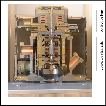
Darmstadt Korrektor
As an illustration this photo shows the so-called "Darmstadt Corrector".
It was based on a Siemens 102 microscope, which had at that time (late 1970s) the highest stability of all commercially available transmission electron microscopes. This was mainly due to its diameter of 30 cm. It was driven at an acceleration voltage of 40 kV. In the upper part the objective lens is situated, below you find the corrector.
First the corrector consisted of five 8-pole elements. The picture shows the final version, where the central 8-pole was substituted by a 12-pole element offering further improvement (eliminating fifth order aperture aberration).
It was shown to be able to correct chromatic and spherical aberration. [See also: Haider M., Bernhard W. and Rose H. (1982): Design and test of an electric and magnetic dodecapole lens Optik 63, 9-23]
detection systems
- fluorescent screen
- The image can be directly observed on such a screen, which is excited by cathodoluminescence, it consists for example of ZnS powder.
- emulsion
- Since the emulsion is directly exposed to the beam inside the microscope vacuum the emulsion has to be dehydrated immediately before using it.
- imaging plate
- Such a plate consists of a thin layer of phosphor on a plastic support. The exposure to the electrons generates luminescence centres. Afterwards the plate is scanned with a He-Ne-laser and the emitted light is registered by a photomultiplier. The plate can be reused. Its sensitivity is about three magnitudes larger than that of a photographic emulsion.
- CCD cameras
- A direct recording of the twodimensional pixel array is very useful for further digital processing and for the beam alignment. Such a camera consists of 10242 up to 40962 photodiodes, each with an area of 20x20 µm2. Since this camera can only register photons one has to use a thin scintillator for the conversion, which is coupled to the camera by using for example a fiber plate. Cooling the camera by a Peltier element improves the signal to noise ratio and allows longer registration times.