
BCOR - Cs/B3 TEM-corrector for aberration-corrected TEM imaging using large scale fields of view
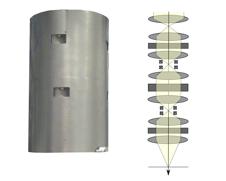
BCOR - Cs/B3 TEM-corrector for aberration-corrected TEM imaging using large scale fields of view
After successful Cs-correction (spherical aberration C3) the off-axial coma is the next intrinsic round lens aberration, which limits the resolving power of the TEM. This is particularly true for large fields of view, e.g. in TEM images by large detectors such as 4kx4k cameras or even larger. The BCOR had been designed to correct for both, the spherical aberration C3 as well as the off-axial coma B3. This enables aberration-free imaging even in the outer corners of of a large detector's field of view. The optimized corrector setup allows for correction of all parasitic(+) axial aberrations up to including 4th order and all off-axial aberrations up to including 3rd order. The BCOR design was carefully verified to avoid intrinsic(++), higher order residual off-axial aberrations and moreover allows for complete correction of the 5th order.six-fold astigmatism. In fact, the BCOR is the first corrector that realizes full "aplanatic" imaging in TEM.The BCOR has proven its capabilities in the field of materials science as well as in life science applications (e.g. single particle reconstructions) in that the whole recorded field-of-view is free from all dominant aberrations. This is especially useful in combination with very large camera systems (4k x 4k and larger).
(+) parasitic aberrations = aberrations that occur due to tolerances and uncertainties in the mechanical build-up of the corrector.
Features:
- Hexapol-type Cs/B3-corrector for TEM
- Correction of the off-axial coma B3 and of all parasitic off-axial aberrations up to including 3rd order, for resolution improvement in the outer image area.
- Correction of all axial aberrations up to 5th order (We, C1, A1, B2, A2, C3, S3, A3, A4, B4, D4, A5)
- Enables real "aplanatic" imaging in TEM
- Information limit better than 70pm at 300kV
- Compatible with the following TEMs: Hitachi HF-3300S, TFS Titan/Krios. Others on request.
Specifications:
- Dimensions: 434 x 390 x 279 [mm]
- Mode: TEM
- High-voltage area: 60kV – 300kV
Applications:
For high-resolution TEM, especially for image acquisition with very large detectors (4k x 4k and larger) for material science as well as for life science applications.
Contact
Do you have any questions about the product or the application and extension for your e-beam system? Please contact us at info@ceos-gmbh.de
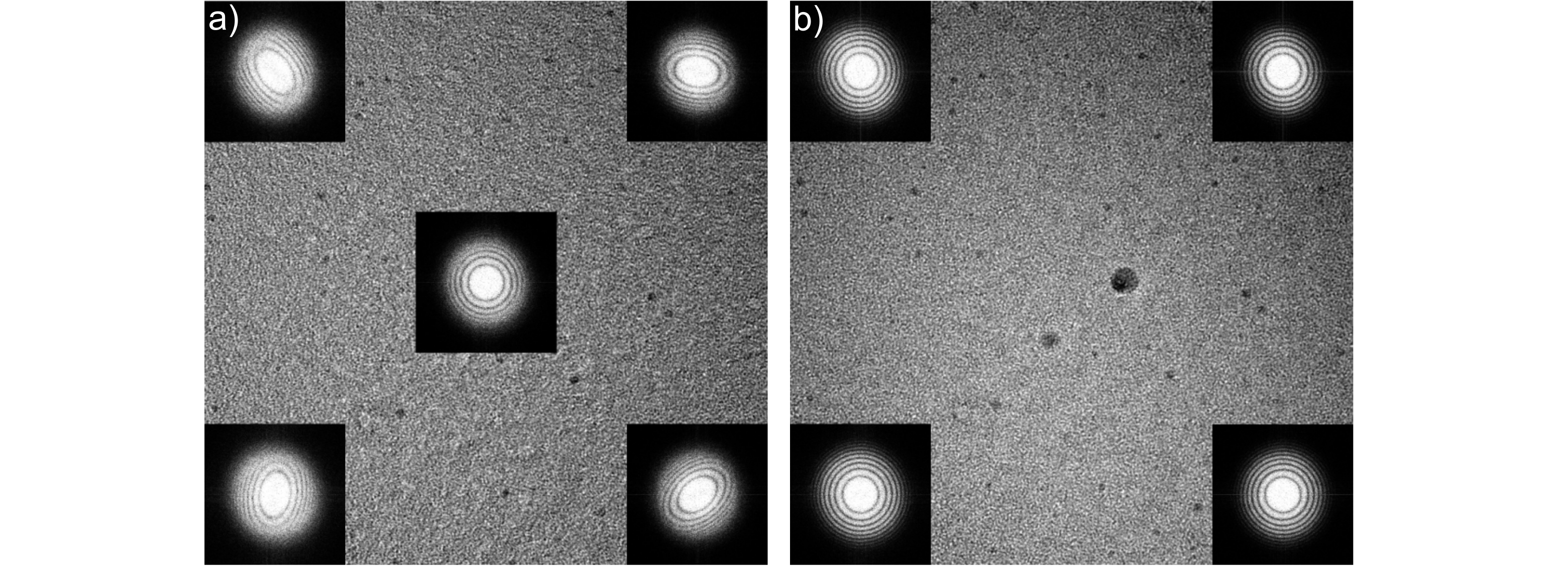
Illustration of the impact of off-axial aberrations: a) uncorrected off-axial astigmatism: the two-fold astigmatism changes quite considerably within the field of view and therefore limits the microscope resolution depending on position in the image. b) After correction of all linear off-axial aberrations up to 3rd order with the BCOR the imaging condition is identical in the whole field of view. The sample is an amorphous tungsten film and images were acquired with a CCD camera (2k x 2k , gNy= 5.36/nm, FoV 191nm x 191nm) in a Hitachi HF-3300 TEM with cold FEG at 300kV.
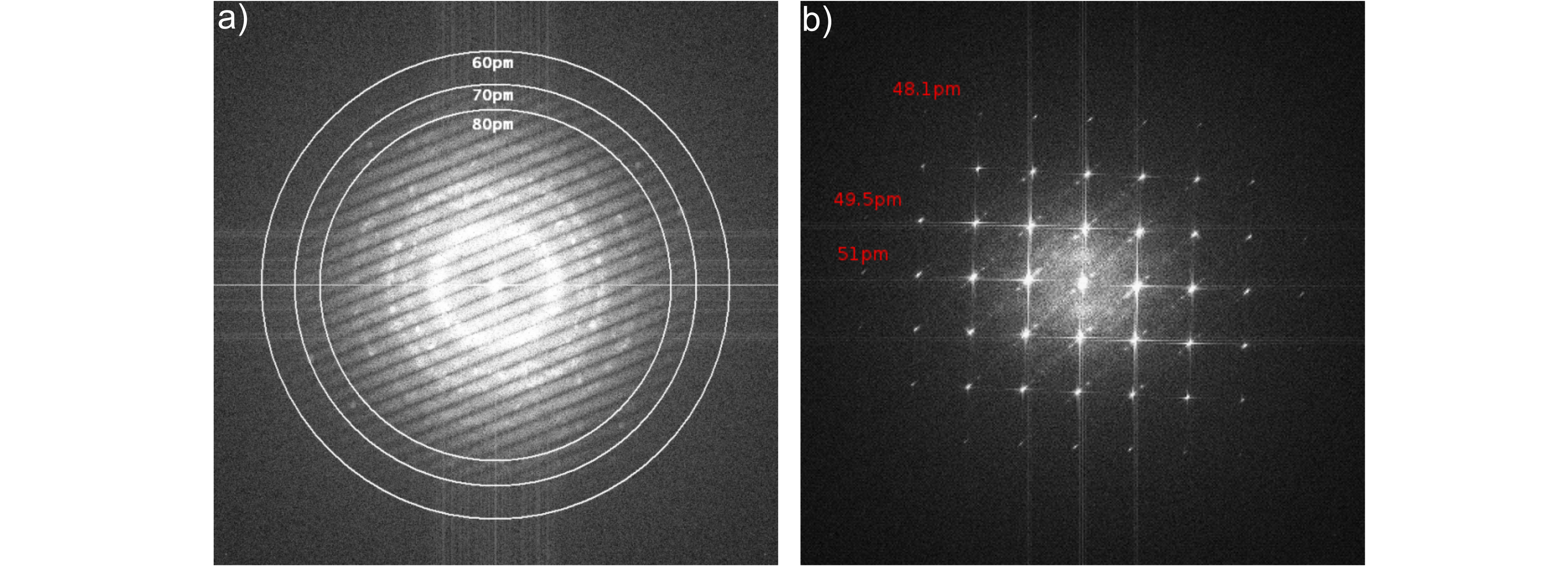
a) Young's Fringes resolution test at a Hitachi HF-3300 TEM with BCOR at 300kV using a thin tungsten film. The sub-70pm information limit is clearly visible. b) The diffractogram of an image of oriented gold (Au [100]) correspondingly shows the very high diffraction orders.
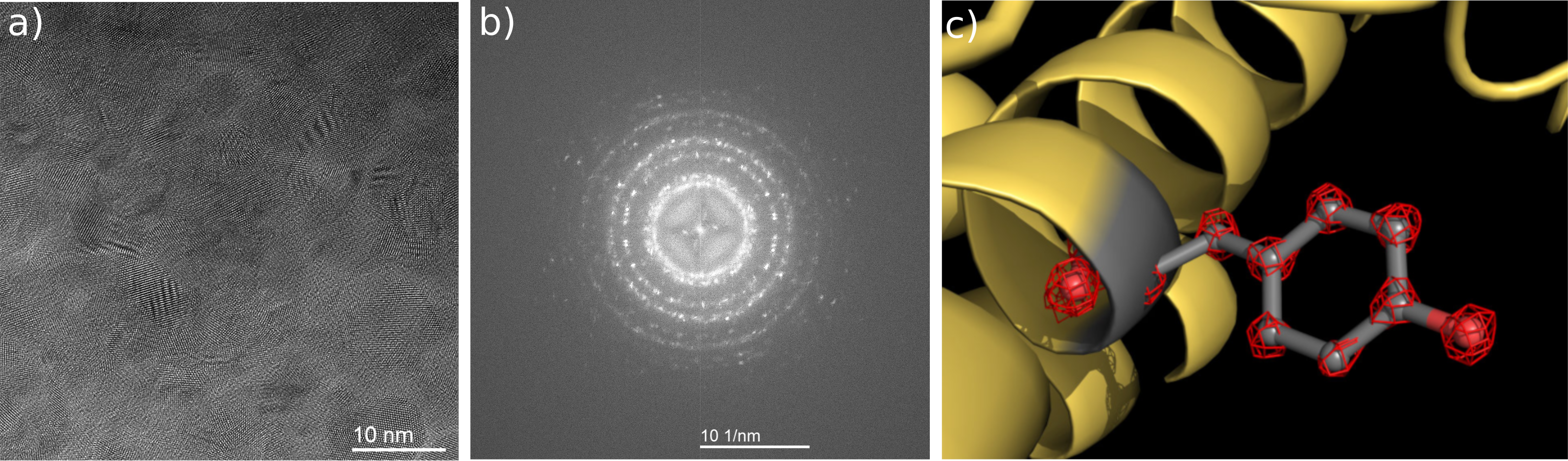
The BCOR by CEOS enables a new resolution record in cryo-electron microscopy: a) The image of gold particles at 300kV was recorded in a ThermoFisher Cryo-TEM with BCOR using monochromated illumination. It demonstrates the outstanding resolving power of the corrected electron microscope. A fast detector allows for accumulation of drift-corrected sub-images over the total acquisition time of 20 sec. b) The research group of Prof. Holger Stark was able for the first time to resolve individual atoms in a proteine structure using cryo electron microscopy. The cartoon-visualization shows a part of an Apoferritin proteine (yellow), where a Tyrosin side-chain is emphasized in grey. The amino acid Tyrosin consists of several atoms, which are individually visible in the structure (red lattice structures). Ka Man Yip, Niels Fischer, Elham Paknia, Ashwin Chari, Holger Stark: Atomic-resolution protein structure determination by cryo-EM. Nature, October 21, 2020.