
CESCOR - Cs-corrector for STEM
CESCOR – Cs corrector for STEM
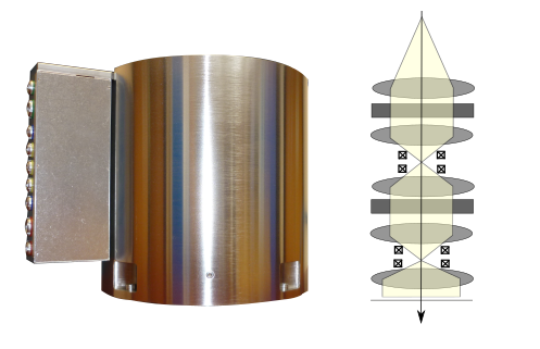
The CESCOR has been designed for the compensation of spherical aberration (Cs) in scanning-transmission electron microscopy (STEM). It is a hexapole-corrector with two multipole stages and it compensates all aberrations up to 3rd order. The first remaining intrinsic aberration (+) is the six-fold astigmatism (A5). The spherical aberration of 5th order (C5) can be adjusted with positive as well as with negative values. The CESCOR can be used variably with accelerating voltages between 80kV and 300 kV. This Cs-corrector permits a high flux in the electron probe. This leads to a 10x higher probe current and at the same time to a 2x smaller probe diameter on the sample as for a non-Cs-corrected STEM microscope. Due to the correction of the spherical aberration (Cs) the probe diameter d59 (++) can be reduced to 0.08 nm at 200 kV. The CESCOR is especially suitable for high-resolution STEM in material science applications in the nano sciences. You can find more information about the CESCOR corrector in our publication:
(+) intrinsic aberrations = aberrations that occur and are unavoidable due to the optical design of the corrector.
(++) The probe size criterion is related to the probe current and is called dp (0<p<100), where p is the fraction in percent of the total probe current contained within a disk of diameter dp. d59 = 0.61(λ/ν) corresponds to the Rayleigh criterion for an Airy function (diffracted limited regime) as basis for the two-dimensional current distribution in the electron probe. Here λ is the wavelength and ν is the probe semiangle.
Features :
- Cs-corrector for STEM (replaced by ASCOR / DCOR)
- Hexapole corrector (2x Hex)
- adjustable aberrations: C1, A1, B2, A2, C3, S3, A3, D4, C5
- Limiting residual aberrations: A5 (intrinsic), A4/B4 (parasitic)
- Highly increased probe current (10x) compared to a non-Cs-corrected STEM.
- Compatible with the following STEMs: TFS, JEOL, Zeiss, Hitachi
Specifications:
- Device dimensions: 255 x 337 x 255 [mm]
- Mode: STEM
- High voltage range: 20kV – 80kV
Applications:
- High resolution STEM for material science in the nano-sciences
Contact
Do you have any questions about the product or the application and extension for your e-beam system? Please contact us at info@ceos-gmbh.de
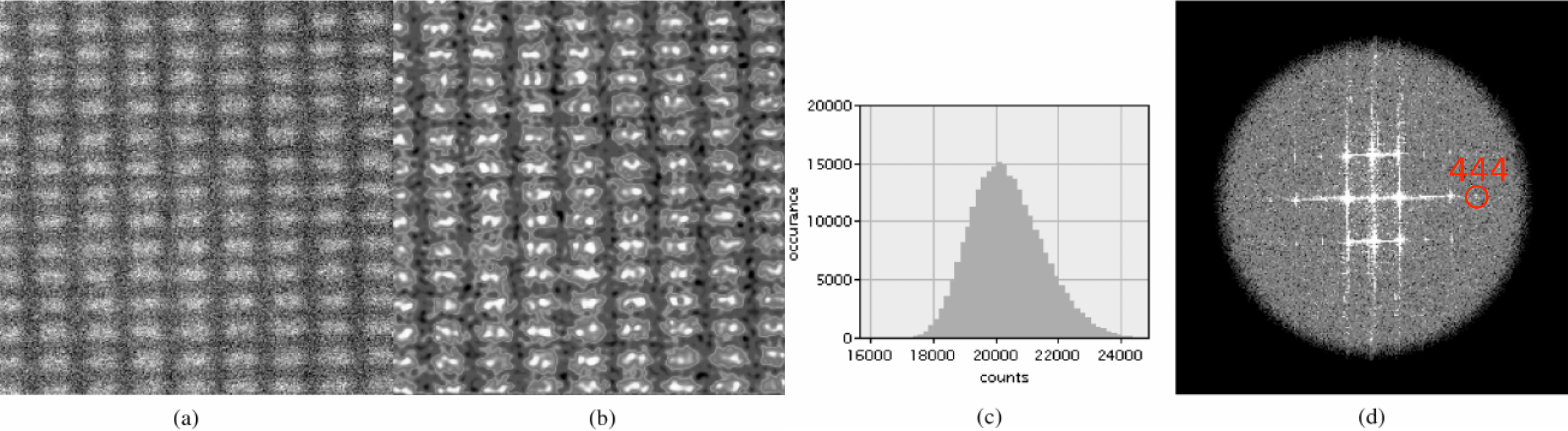
a) Raw data of a STEM ADF image of Si [112], recorded with a CESCOR STEM corrector in a FEI TITAN 80-300 electron microscope at 300 kV. b) For noise-supression the image data has been low-pass filtered, which allows for directl identification of the two individual atomic columns within the dumbell structure that are separated by 78 pm only. The histogram c) shows that the dark-field detector signal was not cut out. d) The Fourier transform of b) clearly shows the (444) reflection which directly corresponds to the 78 pm spacing. Müller et al. Microsc. Microanal. 12, 442-455, 2006.
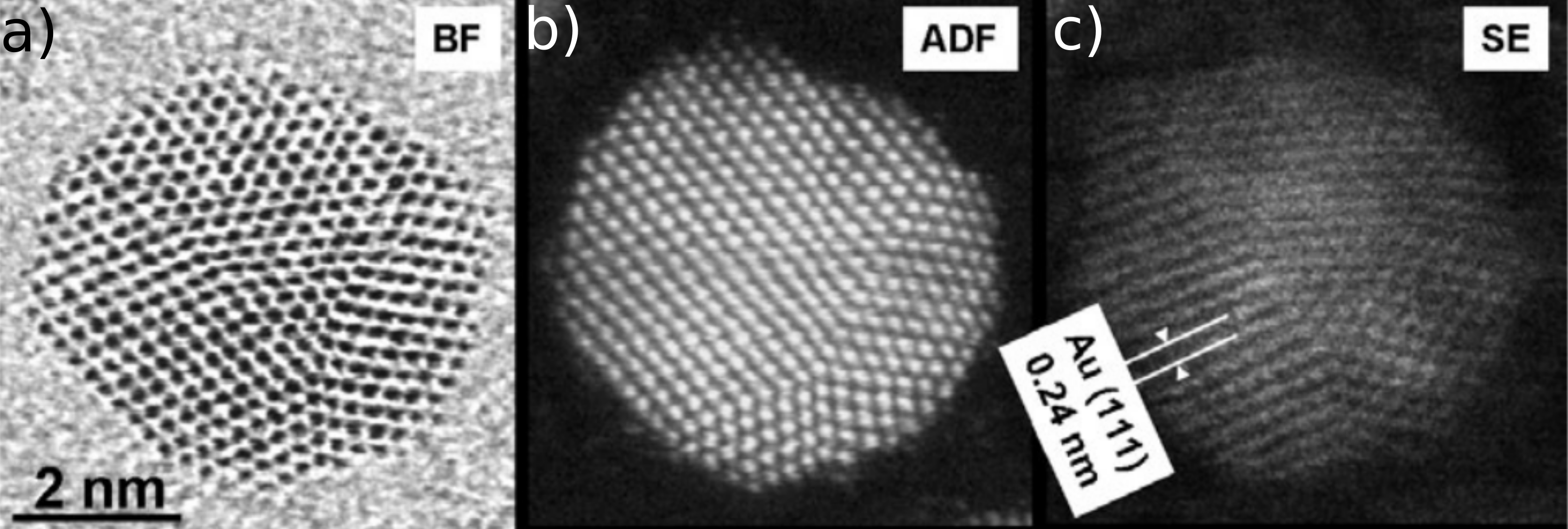
a) Bright-field (BF), b) annular dark field (ADF) and c) secondary electron (SE) images of gold nano-particles. The three images were recorded simultaneously in a Cs-corrected Hitachi HD-2700 STEM/SEM with CESCOR corrector at 200 kV. The probe diameter of about 0.1 nm allows clearly imaging the Au [111] lattice planes with 0.24 nm plane distance in all three detector signals. XF Zhang - Microscopy Today, 2011