
CETCOR-MeV – Cs corrector for TEM (MeV range)
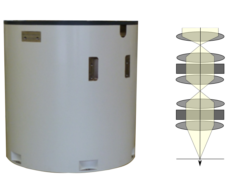
CETCOR-MeV - Cs corrector for TEM (MeV range)
The CETCOR-MeV is a variant of our CETCOR especially developed for the use in transmission electron microscopy up to the MeV range. The CETCOR-MeV compensates the sperical aberration (Cs) and all aberrations up to 3rd order (A1, B2, A2, C3, S3, A3). The CETCOR-MeV can be used for a high voltage range between 400 kV and 1200 kV. At 1200 kV in combination with a cold-FEG, an information limit of 44pm is reached. The CETCOR-MeV is most appropriate for high-resolution-TEM on atomic scale for material science.
Specifications:
- Hexapole-type Cs-corrector for high-resolution-TEM up to the MeV range
- Auto-correction of all axial aberrations up to 3rd order (A1, B2, A2, C3, S3, A3)
- Vanishing delocalisation
- In combination with a cold-FEG an information limit better than 44 pm (at 1200kV) is reached
- Compatible with the following TEMs: Hitachi 1.2MeV ultra-high-voltage electron microscope. Other systems on request.
Specifications:
- Device dimensions: 600 x 702 x 702 [mm]
- Microscopy mode: TEM
- High voltage range: 400 - 1200kV
Application:
High resolution Transmission electron microscopy (TEM) with high accelerating voltages from 400kV up to 1200kV, especially in the field of material science, for particularly thick samples and heavy elements.
Contact
Do you have any questions about the product or the application and extension for your e-beam system? Please contact us at info@ceos-gmbh.de
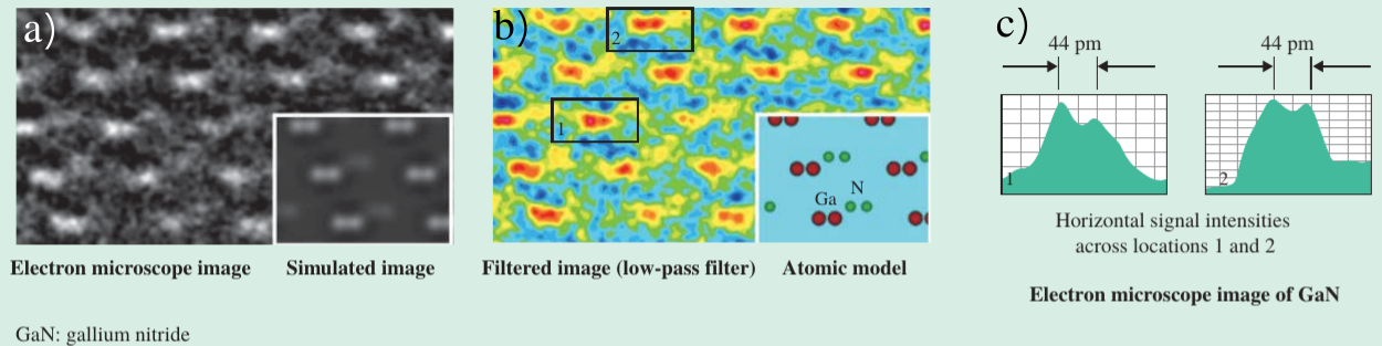
Images of atomic resolution GaN atoms. The images were recorded at 1.2 MeV with a CETCOR installed in a Hitachi 1.2 MeV cold-FEG TEM: Image a) shows the projected atomic localization in GaN [411] with a separation of 44 pm between Ga atoms. The small inset image shows the corresponding simulation image. Image b) shows the same image but filtered with a gaussian low-pass filter and color-coded for image intensity. The inset shows corresponding atomic positions for Ga (red) and N (green) atoms. Image c) shows line profiles along the Ga atom pairs marked with black boxes and numbers 1 and 2 in b). The 44 pm distance between the Ga atoms can clearly be resolved. (Development of Holography Electron Microscope with Atomic Resolution. Hiroyuki Shinada, Hitachi Review Vol. 64 (2015), No.8).