
CETCOR - Cs Corrector for TEM
CETCOR - Cs corrector for TEM
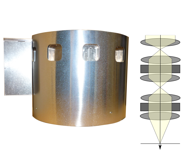
The CETCOR has been designed for the compensation of spherical aberration (Cs) in high-resolution transmission electron microscopes (TEM). The corrector compensates all aberrations up to including 3rd order (A1, B2, A2, C3, S3, A3). The CETCOR can be used variably with accelerating voltages between 30 kV and 300 kV. Due to the correction of image aberrations the point resolution can be matched to the information limit of the TEM. In modern field emission TEMs, the use of a corrector can improve the point resolution by a factor of two compared to the uncorrected TEM. In combination with a monochromized electron gun an information limit of 80 pm (at 200 kV) and 50 pm (at 300 kV) can be reached. The CETCOR is especially suitable for atomic scale resolution TEM of material science applications in the nano sciences.
Features:
- Hexapole-type Cs-corrector for high-resolution TEM
- Auto-correction of all axial aberrations up to including 3rd order (A1, B2, A2, C3, S3, A3)
- Vanishing delocalization in the image
- Improved point resolution
- The combination with a monochromator improves the information limit to 80 pm at 200kV and to 50 pm at 300kV.
- Compatible with many TEMs: TFS (Tecnai F20, Titan, Themis und Spectra), JEOL (JEM-2100F, JEM-2200FS, JEM-ARM200F und JEM-ARM200F NEOARM), Zeiss (Libra 200)
Specifications:
- Device dimensions: 250 x 396 x 306 [mm]
- Microscopy mode: TEM
- High voltage range: 30kV – 300kV
Application:
High resolution transmission electron microscopy, especially in the field of material science.
Contact
Do you have any questions about the product or the application and extension for your e-beam system? Please contact us at info@ceos-gmbh.de
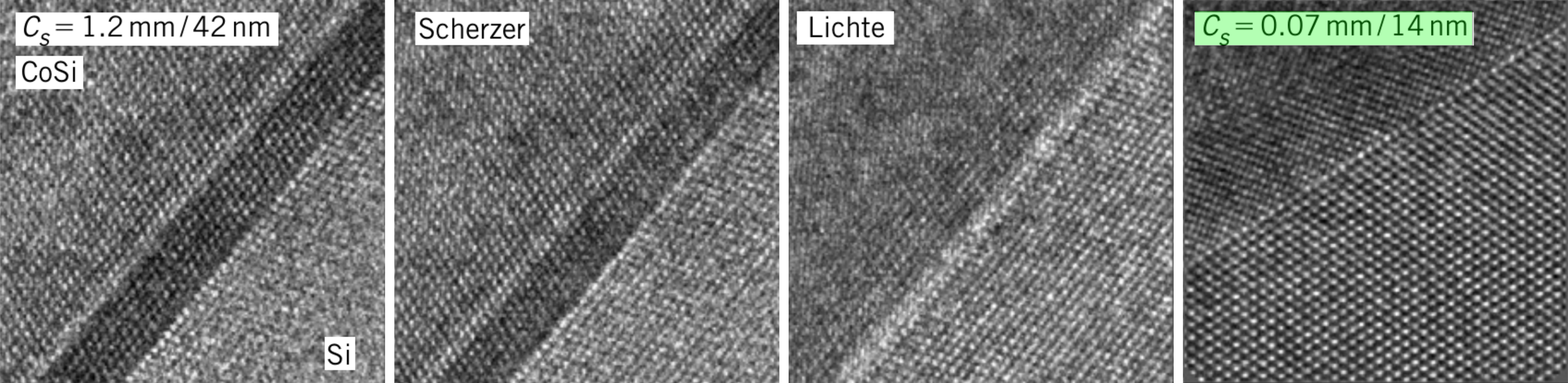
Images of a CoSi2 boundary layer, imaged in uncorrected TEM, at Scherzer focus, at Lichte focus and in Cs corrected TEM. At Lichte defocus the delocalisation can be reduced, but it cannot be eliminated. Only in the Cs corrected case the boundary layer between the elements is imaged with atomic resolution. Images were recorded at 200 kV in a Philips CM200F with the CETCOR switched off and on. (Haider et al., Advances in imaging and electron physics, Vol. 153, p.43-120,(2008)).
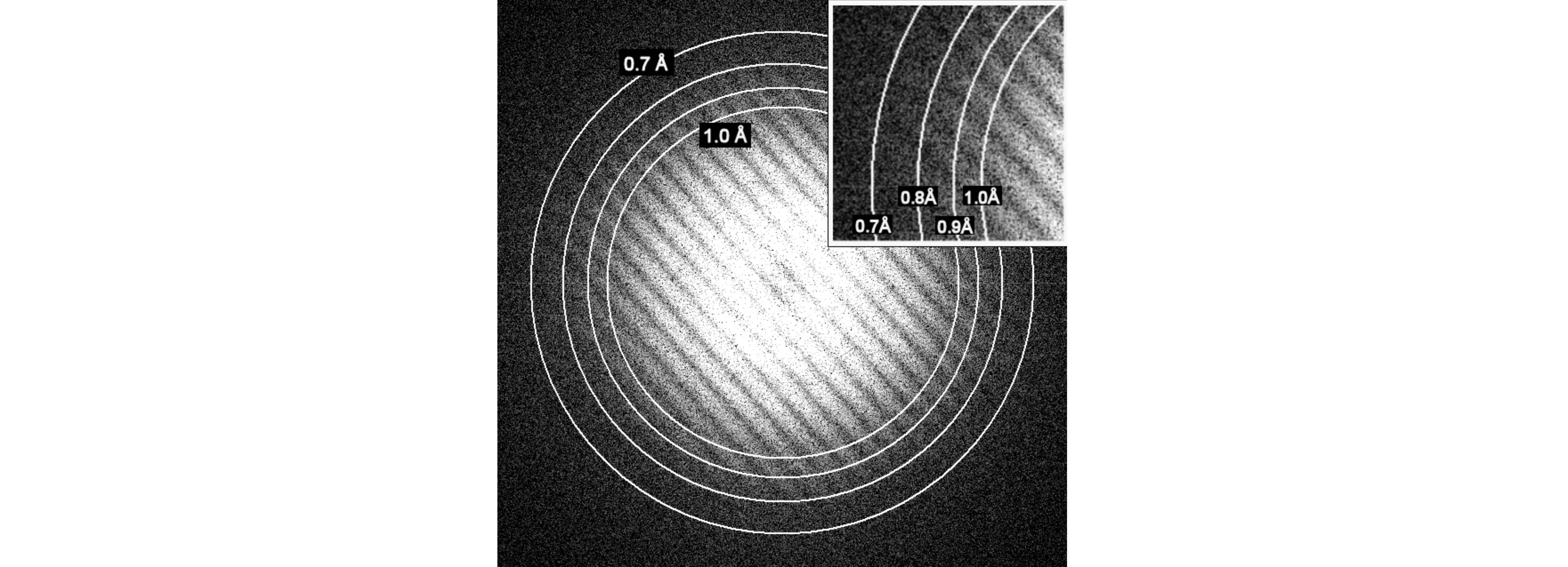
Young's fringes resolution test in a Zeiss UHRTEM with CEOS CETCOR and CEOS gun monochromator (Uhlemann, S., and Haider, M. (2002). Experimental set-up of a fully electrostatic monochromator for a 200 kV TEM. In Proceedings 15th International Congress on Electron Microscopy, vol. I., pp. 327–328. Durban: Microscopy Society of Southern Africa). It demonstrates an information limit of better than 80 pm (or 12.5/nm) at 200 kV. The diffractogram belongs to the image of an amorphous β-tantalum sample. (Schlossmacher et al., Breaking through the Barrier, Imaging & Microscopy 2/2005, 50–52).
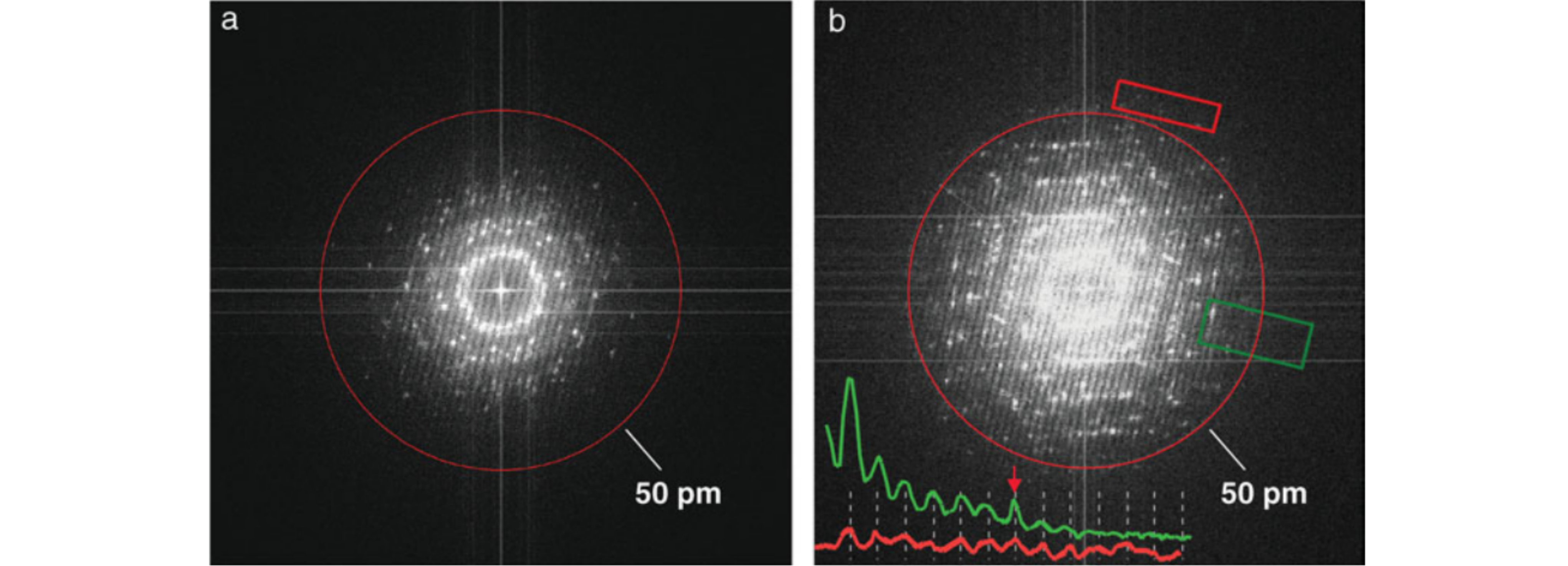
Young's fringes resolution test using an amorphous carbon sample with gold particles. The images have been recorded using a FEI Titan operated at 300kV with high-brightness Schottky-type FEG and the CEOS CETCOR aberration corrector (TEAM 0.5 project). Without monochromator (a) the Young's fringes reach only beyond 70 pm. With monochromator (b) Young's fringes beyond 50 pm (red circle) can clearly be detected. This demonstrates a 50pm resolution with the CETCOR. Line traces (red and green) are taken from areas marked with red and green boxes. The arrow marks the 50 pm position. (From: Kisielowski et al., Microscopy and Microanalysis 14.5 (2008): 469.)